- From the first Hummingbird to the Exynos 8, the family has gone from simple Cortex-A8 to Octa and Hexa designs with big.LITTLE and advanced Mali GPUs.
- The Exynos 7 and 8 consolidated the transition to ARMv8 and 64 bits, introducing their own cores, LPDDR4 memory and powerful GPUs for gaming.
- The new generation with Exynos 2500 and 2600 focuses on 3nm and 2nm nodes, local AI, Ray Tracing and better thermal management to compete with Snapdragon.
- Samsung diversifies with Exynos Auto platforms for connected cars and infotainment systems, strengthening its business beyond mobile.
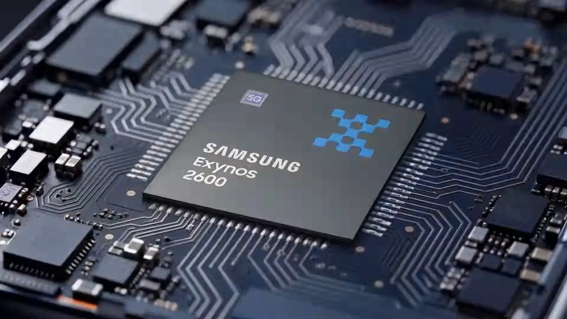
Samsung Exynos processors have become one of the most influential SoC families in the Android ecosystem, both for their role in Galaxy devices and their growing presence in other sectors such as automotive. Over more than a decade, they have evolved from simple mobile chips to complete platforms with advanced graphics capabilities, 5G connectivity, and on-device artificial intelligence.
Today, when you look for detailed information about Exynos , it's no longer just about comparing a specific model to Snapdragon , but about understanding how the architecture has evolved, why Samsung has had periods of success and failure, and what the leap to 3nm and 2nm processes means with the Exynos 2500 and 2600. Let's review that history, the key technologies, and where Samsung stands in terms of competing against Qualcomm and Apple.
From Hummingbird to Exynos: the family's first steps
The origins of Exynos date back to 2010, when Samsung launched the S5PC110 chip, better known as Hummingbird and later renamed Exynos 3 Single . This SoC debuted in the iconic Samsung Galaxy S and included a single-core ARM Cortex-A8 CPU running between 1,0 and 1,2 GHz, accompanied by a PowerVR SGX540 GPU at 200 MHz.
In terms of memory, that first Exynos 3 Single supported dual-channel 32-bit controllers with support for LPDDR, LPDDR2, and DDR2 , a very advanced configuration for the time that allowed for remarkable bandwidth in a 45nm manufacturing process. It was the starting point of a proprietary processor strategy that, over time, would become a key component of Samsung's mobile business.
The real leap into the high-end market came in 2011 with the Exynos 4210, later renamed the Exynos 4 Dual 45 nm , integrated into the Samsung Galaxy S II. This SoC featured a dual-core CPU based on Cortex-A9 between 1,2 and 1,4 GHz, accompanied by a Mali-400 MP4 GPU, and had a very important feature: its controller was integrated into the Linux kernel , with official support from version 3.2 in November 2011.
A few months later, on September 29, 2011, Samsung unveiled the Exynos 4212, later known as the Exynos 4 Dual 32nm . Also based on the Cortex-A9, it increased the frequency to 1,5 GHz and significantly improved the graphics with a Mali-400 MP4 at 400 MHz, resulting in an increase of around 50% in 3D performance compared to the 4210. Furthermore, the move to the 32nm HKMG node brought improved energy efficiency.
The Exynos 4 and Exynos 5 era: more cores, more power, and new features
In April 2012, Samsung introduced the Exynos 4 Quad (Exynos 4412) , which was integrated into the Samsung Galaxy S III and Galaxy Note II. This chip featured four Cortex-A9 cores clocked between 1,4 and 1,6 GHz, with a Mali-400 MP4 GPU running at up to 533 MHz, and a 64-bit (2×32-bit) dual-channel memory bus at 400 MHz compatible with LPDDR, LPDDR2, DDR2, and DDR3.
The company boasted at the time that the Exynos 4 Quad consumed approximately 20% less power than the SoC in the Galaxy S II, despite having an increased number of cores. It was also around this time that Samsung reorganized its naming convention: the old Exynos 3110 became the Exynos 3 Single; the 4210 and 4212 were grouped together as the Exynos 4 Dual (45nm and 32nm); and the 5250 was renamed the Exynos 5 Dual.
Within this same generation appeared the Exynos 4415, another quad-core variant based on Cortex-A9 manufactured on HKMG's 28nm process, with CPU frequencies around 1,5 GHz and a Mali-400 MP4 GPU at 533 MHz. It retained a 64-bit dual-channel LPDDR/LPDDR2/DDR3 memory interface and a bandwidth of around 6,4 GB/s, sufficient for the mid-range/high-end devices of 2014 where it was used.
The major technological leap within the family came with the Exynos 5250, commercially known as the Exynos 5 Dual . Released around the third quarter of 2012 and manufactured using HKMG's 32nm process, it was one of the first SoCs on the market to adopt high-performance Cortex-A15 cores at 1,7 GHz and a Mali-T604 MP4 GPU at 533 MHz, offering significantly superior graphics performance compared to the Mali-400 MPx of the previous generation.
In terms of memory, this Exynos 5 Dual offered bandwidth of up to 12,8 GB/s with LPDDR3 or DDR3 at 800 MHz in a 64-bit dual-channel configuration, or 8,5 GB/s with LPDDR2 at 533 MHz. It supported WQXGA (2560×1600) resolution, Full HD video playback at 60 fps, and modern interfaces for the time such as USB 3.0 and SATA 3, making it a very attractive chip for tablets and productivity devices.
big.LITTLE, Exynos 5 Octa and the first high-performance hybrids
With the maturation of the ARMv7 architecture, Samsung opted for the big.LITTLE approach: combining powerful cores with efficient cores in a single SoC. The first example was the Exynos 5 Octa 5410, manufactured using the 28nm HKMG process, which combined four Cortex-A15 and four Cortex-A7 cores in a 4+4 configuration.
The Exynos 5410 offered frequencies of up to 1,6 GHz on the Cortex-A15 cores and 1,2 GHz on the Cortex-A7 cores , employing an initial big.LITTLE architecture that would later evolve towards more flexible execution modes. For graphics, it used a PowerVR SGX544MP3 GPU at 480 MHz (up to 532 MHz in certain full-screen applications), with a 64-bit dual-channel LPDDR3 memory bus at 800 MHz (up to 12,8 GB/s). It was launched in 2013 and marked the commercial debut of the Exynos 5 Octa series.
Shortly after, the Exynos 5420 and 5422 appeared, also under the Exynos 5 Octa umbrella . They maintained the combination of four Cortex-A15 and four Cortex-A7 cores but raised the bar: the 5420 reached 1,9 GHz on the A15s and 1,3 GHz on the A7s, while the 5422 reached up to 2,1 GHz on the larger cores and 1,5 GHz on the smaller ones. Both integrated a Mali-T628 MP6 GPU at 533 MHz, which translated to approximately 102,4 GFLOPS in single-precision computing.
These SoCs incorporated dual-channel 64-bit LPDDR3/LPDDR3e or DDR3 memory up to 933 MHz, with bandwidths close to 14,9 GB/s, and improved power management thanks to a more refined big.LITTLE execution (with Global Task Scheduling). They arrived on the market between 2013 and 2014 and were used in high-end smartphones and tablets.
Within that same family also appeared the Exynos 5430, an Exynos 5 Octa manufactured on HKMG's 20nm process that maintained the combination of four Cortex-A15 and four Cortex-A7 cores with frequencies of 1,8 and 1,3 GHz respectively. The GPU remained a Mali-T628 MP6, but this time at 600 MHz, raising its theoretical power to around 115,2 GFLOPS. The dual-channel LPDDR3e/DDR3 memory bus at 1066 MHz offered a bandwidth of around 17 GB/s, and it was used in models such as the Samsung Galaxy A7 and A8.
Exynos 5 Hexa and Octa for the mid-range: a balance between power and efficiency
To reach more market segments, Samsung developed variants with fewer large cores but maintaining advanced capabilities. The Exynos 5260, known as the Exynos 5 Hexa , combined two 1,7 GHz Cortex-A15 cores with four 1,3 GHz Cortex-A7 cores in a 2+4 configuration, also featuring big.LITTLE technology and Global Task Scheduling.
The Exynos 5260's graphics were handled by a Mali-T624 MP4 at 600 MHz , delivering performance close to 76,8 GFLOPS in single precision. It retained a 64-bit dual-channel LPDDR3 bus at 800 MHz (12,8 GB/s), positioning it as a very capable mid-to-high-end SoC in 2014, with somewhat lower power consumption than octa-core processors with eight large and eight small cores.
In parallel, the Exynos 5800 was announced , another Octa variant of the 5 series with four Cortex-A15 cores at 2,0 GHz and four Cortex-A7 cores at 1,3 GHz, a Mali-T628 MP6 GPU, and a similar memory bus (dual-channel LPDDR3/DDR3 at 933 MHz). This platform was geared more towards devices with greater sustained processing demands.
Transition to ARMv8 and 64 bits: the Exynos 7
With the arrival of ARMv8-A and the widespread adoption of 64-bit architecture in mobile devices, Samsung launched the Exynos 7 series, designed to take advantage of the new architecture and improve both performance and efficiency. The first model was the Exynos 7 Octa 5433, manufactured using the 20nm HKMG process.
The Exynos 5433 integrated four Cortex-A57 cores and four Cortex-A53 cores (4+4) in Global Task Scheduling mode, with frequencies up to 1,9 GHz in the large cluster and 1,3 GHz in the efficient cluster. The GPU was a Mali-T760 MP6 at 700 MHz, capable of delivering around 142 GFLOPS, supported by dual-channel 64-bit LPDDR3 memory at 825 MHz (approximately 13,2 GB/s). It included an LTE Cat 6 modem and state-of-the-art Wi-Fi and Bluetooth connectivity for the time.
The next big step was the Exynos 7 Octa 7420 , one of the first commercially available 14nm LPE (Low Power Early) chips. It retained the 4×Cortex-A57 + 4×Cortex-A53 configuration, but increased the clock speeds to 2,1 GHz for the larger cores and 1,5 GHz for the smaller ones, and switched the memory to LPDDR4.
The Mali-T760 GPU evolved into an MP8 design in the Exynos 7420, running at 772 MHz and achieving around 210 GFLOPS, with a 64-bit dual-channel LPDDR4 bus at 1553 MHz that provided approximately 24,88 GB/s. This SoC became a market benchmark in 2015 and was key to the reputation of the Galaxy S6 and Note 5.
For lower-end devices, Samsung introduced chips like the Exynos 7 Quad 7570 and the Exynos 7 Octa 7580. The 7570, manufactured using a 14nm process, was based solely on four Cortex-A53 cores (ARMv8-A) and was aimed at the entry-level market, with LTE Cat 4 connectivity and full support for Wi-Fi and Bluetooth. The 7580, produced using the 28nm HKMG process, integrated eight Cortex-A53 cores at 1,5 GHz with a Mali-T720 MP2 GPU at 668 MHz and dual-channel LPDDR3 memory at 933 MHz (approximately 14,9 GB/s), sufficient for a capable mid-range device with LTE Cat 6.
More Exynos 7 variants and the jump to Exynos 8
The Exynos 7 family expanded with models designed to balance cost and performance. The Exynos 7 Hexa 7650 combined two Cortex-A72 cores with four Cortex-A53 cores (2+4), running at 1,7 and 1,3 GHz respectively, and featured a Mali-T860 MP3 GPU at 700 MHz. Like others of its time, it used dual-channel 64-bit LPDDR3 memory at 933 MHz and was paired with LTE Cat 6 modems.
Another important member was the Exynos 7 Octa 7870 , manufactured using a 14nm LPP process, with eight Cortex-A53 cores at 1,7 GHz, a Mali-T830 MP2 GPU at 700 MHz, and dual-channel LPDDR3 memory at 933 MHz (14,9 GB/s). It was designed to offer excellent battery life with very respectable performance for everyday tasks and moderate gaming.
In the next tier up was the Exynos 7 Octa 7880 , also built on a 14nm LPP process, which combined Cortex-A72 and Cortex-A53 cores in a 4+4 configuration. The A72 cores reached 1,88 GHz and the A53 cores 1,3 GHz. The Mali-T860 MP4 GPU at 950 MHz delivered around 71,4 GFLOPS, with dual-channel LPDDR3 memory at 1033 MHz that maintained a bandwidth close to 14,9 GB/s.
The most ambitious leap in that generation was the Exynos 8 Octa 8890 , the first chip in which Samsung dared to use its own custom cores (Exynos M1 “Mongoose”) alongside Cortex-A53 cores in an ARMv8-A architecture. Manufactured using a 14 nm LPP process, it employed a 4×Exynos M1 + 4×Cortex-A53 configuration with frequencies of up to 2,6 GHz (when 1-2 M1 cores were active) or 2,3 GHz (3-4 cores), while the A53 cores remained around 1,6 GHz.
The Exynos 8890's GPU was a Mali-T880 MP12 clocked at 650 MHz , delivering approximately 265,2 GFLOPS of performance, supported by a dual-channel LPDDR4 memory bus running at 1794 MHz (around 28,7 GB/s). The result was a very powerful SoC for its time, used in the Galaxy S7 series, capable of competing head-to-head with the high-end Snapdragon processors of the era.
Exynos vs Snapdragon: Overview and Key Advantages
Beyond specific models, it's worth understanding what Exynos brings to the table compared to other SoCs like Snapdragon. Generally speaking, Exynos and Snapdragon have focused on tightly integrating the CPU, GPU, 5G modem, and artificial intelligence into a single design specifically created for Galaxy devices.
According to Samsung's official communications, the processor is the "brain" of the phone, responsible for its speed, power, and energy consumption . Its performance affects everything from the overall smoothness of the system and the speed at which apps open, to battery life. The company emphasizes that if the processor is efficient, the user experience improves in virtually every aspect.
In the Android market, two main chip families are commonly discussed: Exynos and Snapdragon . While they share many core technologies (ARM architecture, 5G support, etc.), they differ in their custom cores, camera ISPs, power management, and GPU design. Exynos has been primarily used in Samsung devices but has also appeared in phones from other brands, while Snapdragon is found in most manufacturers' devices.
In recent years, Samsung has emphasized that its high-end Exynos processors incorporate custom GPUs with AMD technology and advanced features such as ray tracing . Along with AMIGO (Advanced Multi-IP Governor) technology, these chips aim to deliver high-quality graphics and console-like performance in demanding games and mixed reality experiences, while dynamically adjusting power consumption to prevent excessive battery drain.
Another key feature is the integration of powerful NPUs (Neural Processing Units) , which allow AI to run locally on the phone. This powers features such as automatic photo and video enhancement, facial recognition, real-time translation, and smarter assistants, reducing latency and eliminating the need to continuously send data to the cloud, thus strengthening privacy.
The recent crisis at Exynos and the bet on the automotive industry
Despite the progress, Samsung's chip division has gone through a difficult period in recent years, with losses and the departure of key clients like Google. Some Exynos processors have failed to match the performance or efficiency of the most advanced Snapdragon chips, leading to decisions such as reserving Snapdragon for certain "Ultra" models.
Recent reports indicate that Samsung's LSI division, responsible for designing Exynos processors, ISOCELL sensors, and 5G modems, recorded losses of nearly 1 trillion won in 2024. Part of that result is related to the inability to integrate the Exynos 2500 into the Galaxy S25 series, which forced a rethink of the roadmap.
To compensate, Samsung is strengthening its presence in other sectors, especially the automotive industry. This strategy includes the Exynos Auto V720, chosen by BMW for the upcoming iX3 , which will be the German brand's first electric vehicle to use this platform. This isn't the first collaboration: models in the 7 Series have been using the Exynos Auto V920 platform since 2023.
The Exynos Auto V720 is manufactured using a 5nm process and is designed for advanced infotainment systems , a field where computing power, connectivity, and multi-screen management are crucial. Harman's (a Samsung subsidiary) acquisition of ZF Friedrichshafen's ADAS unit further strengthens its commitment to driver assistance systems (cameras, radar, critical computing, etc.).
The automotive industry itself is currently experiencing a "software and screen war ." While some manufacturers, like Volkswagen, advocate a return to physical buttons for ergonomic and safety reasons, the reality is that large touchscreens and connected systems are here to stay; and processors like Exynos Auto are a strategic component for Samsung in this context.
Exynos 2500: the foundation of the new generation with local AI
Within this context of reinvention, Samsung has unveiled the Exynos 2500 as its new high-end processor with a strong emphasis on artificial intelligence running directly on the mobile device. Manufactured using an improved 3nm process, this SoC is designed to compete head-to-head with Qualcomm and Apple in the premium segment.
According to the manufacturer, the Exynos 2500 is capable of performing up to 59 trillion operations per second (59 TOPS) in AI tasks , representing an increase of nearly 39% compared to its predecessor. This figure places it among the most powerful chips on the market in terms of AI.
At the heart of this capability is its redesigned NPU (Neural Processing Unit) , which allows it to run complex AI functions without an internet connection. This means faster, more contextual assistants, much smarter image and video editing tools, and biometric and security systems that don't have to send your data to external servers.
In terms of "classic" specifications, the Exynos 2500 features a 10-core CPU and an Xclipse 950 GPU based on AMD technology . This combination ensures power for everyday tasks as well as demanding games, video editing, and augmented reality applications. Furthermore, Samsung has invested years in perfecting its 3nm process, and the arrival of the Exynos 2500 demonstrates that this commitment to the manufacturing node has begun to pay off.
Among the first devices confirmed with this SoC is the Galaxy Z Flip 7 , indicating that Samsung is relying on the Exynos 2500 for a flagship product with very high visibility, leaving behind the rumors that pointed to insurmountable manufacturing problems.
Exynos 2600: the leap to 2nm, generative AI and new Xclipse 960 GPU
If the Exynos 2500 marked a turning point, the Exynos 2600 is Samsung's real game-changer . It's the first commercial chip manufactured on a 2nm node with GAA (Gate-All-Around) technology, beating the 3nm processes used by TSMC, Qualcomm, and Google in their high-end solutions.
The use of GAA allows the transistor's "gate" to completely surround the channel, instead of only one or three sides as with FinFETs. Thanks to this, Samsung claims the Exynos 2600 achieves a significant leap in raw performance and energy efficiency compared to the previous generation, with an increase of around 39% in CPU performance.
At the CPU level, the Exynos 2600 employs a 10-core configuration with ARMv9.3 architecture in a 1+3+6 scheme . The main core is a Cortex-C1 Ultra at 3,8 GHz, supported by three Cortex-C1 Pro cores at 3,25 GHz and six Cortex-C1 Pro cores at 2,75 GHz. This configuration aims to combine very high peak performance with excellent ability to maintain sustained performance.
In terms of graphics, the Xclipse 960 GPU, successor to the Xclipse 950 , makes its debut . Samsung claims it doubles the computing performance of the previous generation and offers 50% more performance in ray tracing, in addition to supporting frame generation and resolution upscaling using AI techniques. All of this is designed for top-tier mobile gaming and demanding mixed reality experiences.
The Exynos 2600 also includes a 32K MAC NPU specifically optimized for generative AI, delivering a 113% performance improvement over its predecessor . This allows for the execution of complex models directly on the device, maintaining privacy and reducing latency, for everything from advanced assistants to intelligent photo and video editing.
Improvements in photography, video and thermal management of the Exynos 2600
In terms of imaging, the Exynos 2600 incorporates a new ISP with AI-based VPS and DVNR technologies . The VPS (Visual Perception System) integrates artificial intelligence directly into the image processor, enabling it to recognize complex scenes or very fine details, such as a subject's blink, and react in real time without significantly increasing power consumption.
The DVNR (Deep Learning Video Noise Reduction) function reduces noise in videos recorded in low-light conditions , also using AI, while maintaining sharpness and detail without the need for larger sensors or additional lenses. This ISP can handle cameras up to 320 MP and work with the AVP codec for video, directly targeting ultra-high-end mobile photography and videography.
One of the most sensitive issues in Exynos history has always been thermal throttling, or performance throttling due to heat . To address this, the Exynos 2600 introduces HPB (Heat Path Block) technology, a thermal block integrated directly into the chip that facilitates faster heat transfer to the heatsink.
According to Samsung, this system reduces thermal resistance by approximately 16% , allowing the SoC to maintain more stable temperatures even under prolonged load (heavy gaming, 8K recording, etc.). The company is so confident in this technology that it has reportedly offered it to competitors like Qualcomm for their own designs.
By combining the improved 2nm process, the ARMv9.3 architecture, the new Xclipse 960 GPU, and HPB, Samsung claims that devices with the Exynos 2600 will be able to offer high and sustained performance, without sudden drops due to overheating , one of the most criticized aspects of previous generations.
Performance of the Exynos 2600 versus the Snapdragon 8 Elite Gen 5
The first leaked tests and records on platforms like Geekbench 6 have allowed for a comparison of the Exynos 2600's graphics performance against the Snapdragon 8 Elite Gen 5. Under the Vulkan API, the Xclipse 960 GPU has shown an improvement of around 8% compared to its own previous results and has come considerably closer to Qualcomm's chip.
In September 2025, the Exynos 2600 achieved scores of around 22.829 points in Vulkan tests . In measurements from January 2026, the score rose to approximately 24.726 points, suggesting significant optimization work on drivers or GPU frequency. Simultaneously, particle physics tests improved from 2.715 FPS to 4.388 FPS (a 61% improvement), and the edge detection test increased by around 51%, indicating that specific bottlenecks in the graphics architecture have been eliminated.
The Snapdragon 8 Elite Gen 5, however, remains slightly ahead with scores close to 25.083-27.700 points in similar scenarios. Nevertheless, the gap between the two has narrowed considerably: where the difference was previously estimated at around 21%, it now stands at approximately 12%, a much more competitive margin for future Galaxy devices.
In Vulkan GPU tests performed on the Galaxy S26 equipped with the Exynos 2600, scores ranging from 19.825 to 24.726 points were recorded . These variations are explained by differences in firmware, performance modes, and cooling settings between prototypes. In any case, the data confirms that the graphics processor is among the best in the market.
Although OpenCL scores have remained more stable, the push in Vulkan, coupled with a previous increase in CPU frequencies estimated at around 12% , paints a picture in which Exynos is no longer so far behind Qualcomm, but becomes a serious alternative in overall performance, AI and efficiency.
Galaxy S26 and the dual chipset strategy
The Exynos 2600 has already been detected in Galaxy S26 prototypes on databases like Geekbench , marking the first time this chip has been seen running in a real phone. Until now, it had only been tested on internal development boards, so these results, while not definitive, provide a fairly clear idea of its performance.
The global version of the Galaxy S26 that appeared in these tests features the Exynos 2600 processor paired with the Xclipse 960 GPU , confirming what was widely expected: Samsung will once again heavily rely on its own chips in various markets. The company has hinted that it will combine the Exynos 2600 and the Snapdragon 8 Elite Gen 5 in the S26 range, depending on the region.
Everything points to South Korea, India, and Europe selling versions with the Exynos 2600 , while other regions will opt for Snapdragon. The Galaxy S26 Ultra, meanwhile, is expected to launch globally only with a Qualcomm chipset, repeating the strategy seen in recent generations.
Beyond the leaks, Samsung has already released a teaser of the Exynos 2600 and officially announced the chip, with a full presentation scheduled for the end of February . All the technical details (final frequencies, exact memory support, video capabilities, etc.) will be revealed then, but the focus on AI, ray tracing, advanced photography, and thermal management is already clear.
The multi-threaded CPU results of the Exynos 2600 in the Galaxy S26 are not yet fully consolidated in public databases, but estimates suggest that it will be able to seriously challenge the Snapdragon 8 Elite Gen 5 , especially in workloads that take advantage of the 10 cores and the L1, L2 and L3 cache improvements that Samsung has been highlighting in its press releases.
This entire journey, from the first Hummingbird to the ambitious 2nm Exynos 2600, paints a picture of a processor family that has had its ups and downs but is now back at the forefront of the industry: chips with 10-core CPUs, Xclipse GPUs with Ray Tracing, NPUs capable of running generative AI locally, advanced ISPs with VPS and DVNR, and a clear focus on thermal efficiency . If the official figures and benchmarks translate into a good user experience in Galaxy devices and new opportunities in the automotive and other sectors, Exynos is poised to regain prominence against Snapdragon and Apple Silicon.
