- A transistor is a semiconductor with three terminals that controls current to amplify or switch signals.
- There are BJTs, FETs (JFET, MOSFET), phototransistors, IGBTs, and configurations such as Darlington.
- Its key parameters (VBE, β, breakdown, power) and the material (Si, Ge, GaAs) determine performance.
- Its impact ranges from microelectronics to power: telecommunications, medicine, automotive and consumer goods.
If today you carry a mobile phone in your pocket, listen to music with a compact system, or connect to the Internet from a ultra-thin computerIt's all thanks to a small but mighty invention: the transistor. Since its emergence in the late 40s, this semiconductor device has driven the miniaturization and power of modern electronics. We'll tell you all about it in detail below. What is a transistor and what is it used for?, how it works internally, what types exist, what parameters really matter and why its history marked a turning point.
Although its basic definition can be summed up in one sentence, its scope is enormous: A transistor controls or modifies the flow of current between two terminals, responding to a signal applied to a third terminal. That's why it serves as amplifier, switch, oscillator or even rectifierFrom a home speaker to a medical scanner. Let's take it step by step.
What is a transistor?
The word transistor comes from the English expression transfer resistor ("transfer resistance"). In practice, it is a semiconductor component with at least three terminals capable of allowing more or less current to pass between two of them depending on what happens in the third. This control over the current or conductance of the channel is what allows weak signals to be amplified or to act as a very fast switch.
In its classic form, the bipolar junction transistor (BJT) has emitter, base, and collectorA small current entering through the base controls a much larger current between the emitter and collector. In the case of field-effect transistors (FETs), the control is achieved by applying voltage to the gate, modulating the conductance of a channel between the source and drain with a very high input impedance.
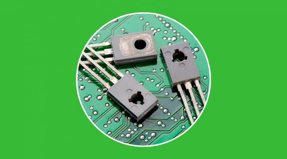
They are mostly manufactured in siliconalthough they also exist in germanium, gallium arsenide (GaAs) or silicon-germanium alloys, massively embedded in integrated circuits (microchips) or packaged as discrete parts. Their encapsulation is usually airtight, with a plastic or metal casing and three pins, and is the basic active element of almost all current electronics.
A bit of essential history
The dream of controlling currents in solid-state devices predates their industrial realization. In 1925, Julius Edgar Lilienfeld registered patents in Canada and later in the US for devices that anticipated the FET, but There was a lack of quality in the semiconductor materials to put them into practice. In 1934, Oskar Heil patented something similar in Europe, and experiments with crystals multiplied. Even so, it wasn't until 1947 that John Bardeen and Walter Brattain, at Bell Laboratories, observed signal gain with two gold points on a germanium crystal.
In the following months, William Shockley delved deeper into semiconductor physics and would propose the bipolar junction transistorThe first patent application for the transistor was filed in 1948. That same year, in France, Herbert Mataré and Heinrich Welker independently developed the "transistron" for the telephone network. Shortly afterward, in 1953, Philco presented the first high-frequency transistor (up to 60 MHz), and in 1954 the first transistor was achieved. silicon operating system at Bell (Morris Tanenbaum) and the first commercial model at Texas Instruments (Gordon Teal).
The next great revolution was the MOSFETBuilt in 1960 by Dawon Kahng and Martin Atalla, it was key to integrating millions of transistors per square centimeter. In recognition of this milestone, Shockley, Bardeen and Brattain received the Nobel Prize in Physics In 1956, he received the Nobel Prize for his research and the discovery of the transistor effect. Since then, electronics has experienced an explosion in the timeline of computer historyFrom portable radios to computers, including telecommunications and medicine.
Structure, signals and how a BJT works
A BJT is made up of three doped regions that create two PN junctionsemitter, base, and collector. They are constructed as NPN or PNP (the middle letter indicates the type of base) and the doping of each zone is carefully controlled: normally the emitter is more heavily doped than the collector. In operation, the collector current is approximately proportional to the base current according to the parameter beta (β) or current gain.
Between the base and the issuer, it behaves as a forward-biased diode, with typical voltage VBE of 0,6-0,8 V in silicon and ~0,4 V in germanium. This diode makes the base the control that opens or closes the flow of charge carriers from the emitter to the collector. Conceptually, the base regulates a "tap" of electrons or holes, so that a small control current manages a larger one at the exit.
Operating modes: active, cut-off, and saturation
The transistor can work as linear amplifier en active regionwhere it allows a flow rate proportional to the base excitation. If the base does not receive sufficient excitation, the device enters court and it doesn't lead. If the excitation is high, it is located in saturation and allows the maximum current permitted by the circuit. This versatility makes it suitable as a fast switch or a weak signal amplifier.
NPN vs PNP in a nutshell
In an NPN, electrons typically flow from collector to emitter and the device is activated by increasing the base current with a positive reference; in a PNP, the practical direction is reversed (emitter to collector) and the biasing logic is complementary, allowing symmetrical configurations in many analog or switching stages.
Types of transistors you will encounter
The family is large, but they all respond to the same idea of controlling the flow of electricity. These are the most common and some historical facts worth knowing:
- Timely contactThe pioneer (1947), with two germanium tips. Difficult to manufacture, fragile and noisy, but it demonstrated the gain for the first time. Today it is a museum piece.
- Bipolar junction transistor (BJT)The classic NPN/PNP transistor on a single semiconductor crystal, doped with donor impurities (arsenic, phosphorus) or acceptor impurities (aluminum, indium, gallium). It is a current-controlled device.
- Field-effect transistors (FETs): JFET (junction gate PN), IGFET and MOSFET (door insulated by rust). They are voltage controlled, with very high input impedance; cornerstone of large-scale integration.
- Phototransistors: light-sensitive, where illumination acts as a base current; perfect for remote detection by electromagnetic radiation.
- IGBTs: insulated gate bipolar, widely used in power by combining advantages of BJT and MOSFET.
- Darlington coupleTwo cascaded BJTs within the same package greatly increase the global gain.
Parameters and materials that make the difference
When choosing a transistor, it's not just the type that matters; its characteristics also matter. electrical parameters: breakdown voltages (collector-emitter, base-emitter, collector-base), maximum power, thermal dissipation, operating frequencyβ, and internal dynamic resistances. In small-signal BJTs, β typically ranges from 100 to 300. The VBE decreases with temperature at approximately a rate of −2,1 mV/°C made of silicon, so there are designs that incorporate sensors or thermal compensation.
Material also matters: the germanium It offers higher mobility than silicon, but its leakage and permissible temperature are worse; silicon It is known for its robustness and ease of manufacture; the GaAs It shines at high frequencies thanks to its electronic mobility. Devices such as the following are based on GaAs/AlGaAs: HEMT, with very low noise and high speed, used in satellite receivers around 12 GHz and, with nitrides, in state-of-the-art power applications.
Another useful way to view a BJT is through the model of Ebers-MollTwo diodes: one base-emitter in forward bias and the other base-collector in reverse bias. This helps to understand why a voltage appears.BE typical (0,6-0,8 V Si) and how it behaves outside the linear region. In JFETs and MOSFETs, the gate voltage is dominant: making the JFET-GS more negative pinches off the channel; in MOSFETs, the gate It does not consume electricity. Ideally in DC, the signal controls the channel conductance between source and drain.
Most commonly used amplifier configurations
With BJTs, it's common to think in terms of three classic topologies. Each one optimizes a quality different (voltage, current or impedances) and that's why they are still in all books and projects.
- common emitterVoltage and current gain, with phase inversion; it's the workhorse. An emitter resistor stabilizes And, if bridged with a capacitor, it recovers AC gain.
- Common collector (emitter follower): voltage gain close to 1, high input impedance and low output; ideal as an impedance adapter.
- Common base: current gain, without phase inversion and very low input impedanceIt shines with low impedance signal sources, such as dynamic microphones in certain setups.
A practical example (polarized common emitter with divider)
Imagine you design a stage with VCC=20 V, ICQ=10 mA, VCEQ=8 V and β=100. If you set the emitter voltage around 1/10 of VCC (2 V), you get RE≈200 ΩThe drop in RC would be VRC=VCC−VCE−VE=10 V, with IC=10 mA, then RC=1 kΩThe base remains at VB=VE+VBE≈2,7 V. If you size the divider with a current about ten times the base current, you get R2≤ 2 kΩ and, in proportion to VCC, R1≈12,8 kΩ.
For small signal, the dynamic resistance of the internal emitter (re) at 10 mA is ~26 mV/I≈2,6 Ω, which gives a voltage gain ideal approximate Av≈−RC/re≈−385. With a 5 kΩ load on the collector, the effective output impedance is around 830 Ω and the gain drops to ≈−319. The impedance seen at the base is re·β≈260 Ω, and the total input resistance, considering a divider and base in parallel, is ≈226 Ω. The coupling and emitter capacitors are chosen so that their reactance is negligible in the work area.
This example summarizes the idea of load line and point Q: you choose a resting point (often V)CE≈VCC/2 without RE) that allows symmetrical signal excursion. From there, you adjust gain, impedance, and stability according to the application.
FET and MOSFET: voltage control
In FETs there is no base current per se, but rather a gate voltage which controls the channel width. The basic JFET starts with a bar of N-type or P-type material, with ohmic contacts at its ends (drain and source) and two diffuse regions that form the gate. As the gate voltage becomes more negative (in an N-type JFET), the channel becomes strangles and the driving stops.
The MOSFET, on the other hand, isolates the gate with an oxide dielectric and achieves a huge input impedance. This, combined with its manufacturing process compatible with integration, explains why it is the chip king modern and why it spurred the generations of processors: allows the integration of hundreds of thousands to billions of interconnected transistors per square centimeter in several layers.
Practical applications: from everyday life to industry
Listing them all is impossible, but it's worth remembering the most representative ones. Such as amplifiersTransistors amplify signals in radios, televisions, or audio equipment. For example... switchesThey control switched-mode power supplies, motor controllers, or lighting systems. oscillatorsThey generate radio frequency signals for communications. And, of course, they are the basic building block of... integrated circuits on computers, smartphones, and all kinds of digital devices.
In the professional sphere, their role is critical in telecommunicationsMedical electronics, industrial automation, or robotics. Their ability to do smaller and more efficient circuits It has changed the way products are designed and manufactured, with more portable, powerful and low-consumption equipment.
Advantages over thermidion valves (and why they are still sometimes used)
Before the transistor, vacuum tubes ruled. But they needed high voltages dangerous, they consumed a lot of energy, they were bulky and heavy (chassis and transformers), they failed more They were prone to overheating and took a long time to reach operating temperature due to filament heating. Furthermore, they suffered from microphonic effects and operated at high impedancesTransistors brought low power consumption, low voltage, compactness, robustness, and lower cost from the beginning.
A historical fact illustrates the difference: the ENIAC, one of the first digital computers, weighed more than 30 tonnes and consumed about 200 kW to power approximately 18.000 valves, with daily breakdowns. Even so, valves survived in specific niches: some high-power radio or audio amplifiers (due to their high-level linearity and the character of its harmonics), hardened equipment against electromagnetic impulses and extreme power applications. Over time, solid-state electronics also conquered many of those frontiers.
Construction features and details
As a general rule, a discrete transistor is a sealed semiconductor device with three visible terminals. It can be configured in stages that function as amplifier, switch, oscillator or rectifierSilicon is preferred in many designs due to its thermal and leakage properties, but there are also germanium families and compounds for specific tasks, such as microwave oven or very high speed.
In BJTs, as the temperature increases, the forward junction voltage decreases and leakage currents can increase, therefore heat dissipation And the choice of maximum power are key. In power FETs, the manufacturing process can create parasitic diodes (like the Schottky between source and drain), something to keep in mind when designing the circuit.
Quick comparison of materials
If you're wondering why some materials are faster than others, think about the mobility of electrons and holes. Ge has high mobilities, but a worse maximum temperature, greater leakage, and lower tolerance to high voltagesSilicon offers excellent balance and typical junction temperatures of 150-200 °C; GaAs raises the bar at high frequencies, although its manufacturing process is more demanding. Therefore, each reigns supreme in its respective segment.
Digital usage: from the perfect switch to logic
In digital switching, a transistor operates by alternating between cut and saturationwhere it ideally behaves as an open or closed circuit. This speed of change and its reduced power consumption make logic gates and the binary systemand, in turn, the CPUs and memories. With MOSFETs and CMOS technology, static power consumption is extremely low because the gate does not drive in DC and is only consumed during transitions.
Practical advantages in installations and devices
For everyday use, transistors are essential. small size (equipment that is easier to transport and integrate), Long useful life (less maintenance), speed (key in processors and communications), low cost (reduces system costs) and Energy Efficiency (lower losses). In a home, everything adds up: from stable regulated sources to automation and savings.
Frequently asked questions that should be answered
Is a transistor only used for amplification? No. It's also a switch ultra-quiet and ultra-fast, a logic circuit brick, a light detector (phototransistor) or part of a oscillatorIts versatility is its greatest advantage.
In which industries is it critical today? Virtually all of them: telecommunications and networksMedical equipment, automotive, energy, manufacturing, and consumer electronics. The combination of power, miniaturization and control has multiplied its impact.
Why do some people talk about "on/off"? It's a colloquial way of referring to states of cut (off) and conduction (whether active or saturated). In practice, these are the logical positions that allow turn on or off the passage of current.
Seventy-odd years after its birth, the transistor remains the heart of electronics: From the first point of contact with germanium to MOSFETs The latest generation can accommodate thousands of milestones, but the core idea hasn't changed: precisely controlling how electricity flows to create stronger, cleaner signals or reliable logic within increasingly smaller spaces.

Table of Contents
- What is a transistor?
- A bit of essential history
- Structure, signals and how a BJT works
- Types of transistors you will encounter
- Parameters and materials that make the difference
- Most commonly used amplifier configurations
- FET and MOSFET: voltage control
- Practical applications: from everyday life to industry
- Advantages over thermidion valves (and why they are still sometimes used)
- Construction features and details
- Quick comparison of materials
- Digital usage: from the perfect switch to logic
- Practical advantages in installations and devices
- Frequently asked questions that should be answered