- Intel 18A incorporates RibbonFET and PowerVia technologies for increased performance and energy efficiency.
- The new node enables higher transistor density and a significant reduction in power consumption compared to previous generations.
- The adoption of Intel 18A positions the company as a leader in semiconductor innovation, impacting numerous sectors such as AI, servers, and mobile devices.
In the fast-paced and ever-changing world of hardware, there are key moments when a technology marks a turning point. The arrival of the Intel 18A node is undoubtedly one of those landmark dates in the tech industry . If you use a computer, mobile phone, or any digital device daily, your routine is about to change, even if you don't notice it at first glance. Intel has gone all in on this new generation of chips, which not only promises to be faster and more efficient but also to lay the groundwork for future developments in artificial intelligence, video games, servers, and many other areas.
But why is everyone talking about Intel 18A? Where did this technology come from, and how does it differ from previous nodes? Let's delve into the intricacies of this quantum leap in semiconductor manufacturing, reviewing all the recent official data, what it means for the competition, and what benefits it will bring to users, both in terms of performance and energy consumption and sustainability.
What exactly is Intel node 18A?
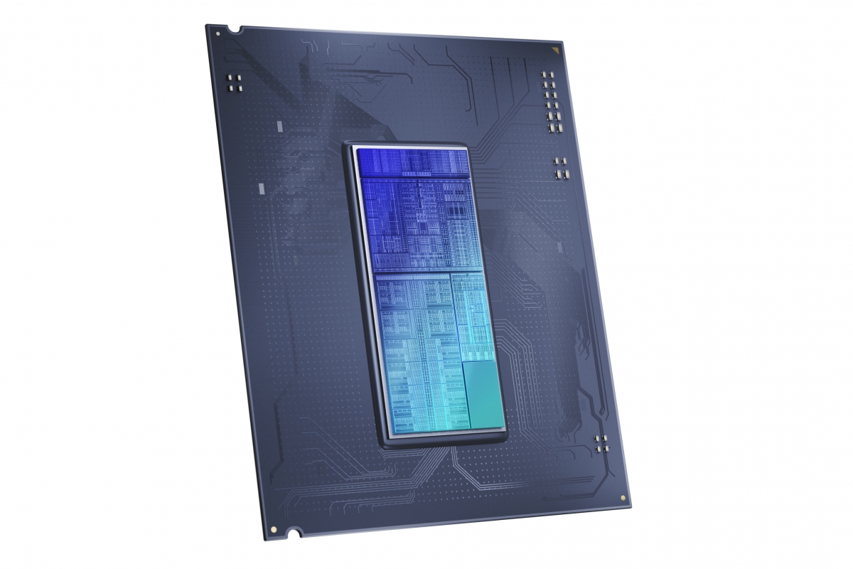
The term Intel 18A identifies a next-generation chip manufacturing technology developed by Intel, and refers to a process size of 18 angstroms (1,8 nanometers). This is significantly smaller than the nanometer-sized nodes that dominated just a few years ago. In practice, this translates to much denser chips, capable of housing more transistors in the same space, which opens the door to higher performance and improved energy efficiency.
We're talking about the new frontier of semiconductor miniaturization . To give you an idea, an angstrom is one-tenth of a nanometer. Previously, the leading nodes were around 7 nm, then 5 nm, and then 3 nm, but now the star is the 18A , competing directly with technologies from TSMC and Samsung. It's not just a matter of size: this node incorporates at least two fundamental technical innovations to improve performance and power consumption.
- RibbonFET (Gate-All-Around): This is a new transistor architecture where the gate completely surrounds the current channel, allowing for greater control of electrical flow. This represents an evolution compared to the three-dimensional FinFETs used until now.
- PowerVia: A revolutionary power distribution system that physically separates power and signal lines, routing power through the back of the chip and freeing up space on the front. This improves density, efficiency, and makes it easier to incorporate more transistors.
Thanks to RibbonFET and PowerVia, Intel 18A marks a substantial leap forward compared to previous nodes such as Intel 7, Intel 4 or Intel 3 , both in terms of the type of transistors and the way they are electrically powered.
A little context: evolution of Intel nodes
In recent years, Intel has undergone a radical transformation in how it names and manufactures its nodes. The old Intel 7 node was widely used from the 12th generation of Core processors, known as Alder Lake, and in subsequent generations (Raptor Lake, 4th generation Xeon Scalable, etc.). This node actually represented the 10nm Enhanced SuperFin technology, but Intel renamed it to differentiate it from TSMC's N7.
Later, Intel 4 represented the true leap to 7nm with EUV (extreme ultraviolet) technology, although it was only present in the Compute Tile of Meteor Lake. Intel 3 was an incremental improvement over Intel 4, primarily in density and efficiency, and was mainly intended for the new Xeon 6 server processors.
From there, the original plan was to move to the Intel 20A node (equivalent to about 2 nm), but this was commercially discontinued in 2024, giving way to a complete focus on Intel 18A . Therefore, 18A is the direct successor and great hope for Intel's survival and leadership in the coming years.
Major customers, such as NVIDIA, are already testing the development of their own chips using Intel 18A technology, confirming its maturity and appeal both within and outside the Intel community.
How does Intel 18A work and how is it really different?
The key lies in how the transistors have been redesigned and in the new way power is distributed within the chip . Modern processors contain billions of tiny transistors, which function as microscopic switches. Until recently, the FinFET architecture was the standard: the transistors were like small vertical fins (hence Fin-FET, Fin Field-Effect Transistor), but they had certain limitations, especially when it came to further reducing size and unwanted effects such as electrical leakage.
With the RibbonFET system , also known as GAA or Gate-All-Around, the channel through which the electricity flows is completely surrounded by the gate, increasing control capacity and minimizing losses and leakage. It's like going from having an open channel (more exposed to leaks) to having it completely enclosed in tubing.
The other crucial improvement is PowerVia . Until now, both the signal and electrical power entered through the same "main door" of the chip. This caused interference and reduced the space available for routing signals and power. Now, with PowerVia, all power supply connections are moved to the back of the silicon, freeing the front for signals only, which allows for more compact and efficient chips.
This double advance translates into faster chips, capable of consuming less energy and with greater stability even in high-performance situations.
What specific improvements does Intel 18A bring compared to previous nodes?
The question everyone is asking: Is the leap from what we already know really noticeable? And, according to official documentation and data shared at recent international events (such as the VLSI Symposium 2025), the answer is affirmative, and quite resounding:
- 30% more transistor density than Intel 3. This means that many more transistors can fit into the same physical space, which is the basis of any improvements in computing and efficiency.
- Up to 25% performance increase over Intel 3 at the same voltage (1,1V in official tests), or 18% improvement even by lowering the voltage to 0,75V.
- Reduction in energy consumption of up to 36% with the same frequency and voltage, and up to 40% lower voltage, compared to Intel 3.
- Advances in electrical stability and interference reduction, essential to ensure reliable operation in high-performance chips.
These values were obtained by comparing them with standard ARM chips, but virtually all processor ranges will see these improvements, from laptops to servers and GPUs.
Impact on products and applications: What devices will use it?
According to the latest leaks and announcements, the first product to arrive with the Intel 18A node will be the Panther Lake family , aimed at next-generation laptops. Shortly after, it should be incorporated into CPUs for high-performance servers, workstations, and, if tests with external clients are successful, it could appear in products from companies like NVIDIA.
At the internal architecture level, in modern processors (for example, Panther Lake), not only the cores can benefit from the 18A node, but also the entire ecosystem of internal components: memory controllers, I/O interfaces, data interconnect systems, etc. This further amplifies the efficiency and performance advantage, not only increasing raw power, but also the overall system's ability to handle more tasks simultaneously.
Furthermore, mass production is planned for the second half of the year, after confirming the maturity and reliability of the process, which allows for wafer manufacturing with a high success rate—a critical factor for any node to be competitive in terms of cost and volume.
The importance of the Intel 18A node for the industry and Intel's future
The industrial context cannot be ignored: Intel has staked its recent future on the viability and success of 18A . After a series of internal crises, the cancellation of intermediate nodes, and pressure from competitors like TSMC and Samsung, the company needs not only to lead in technology but also to inspire confidence in its international investors and customers.
The steady development of 18A allows Intel to regain the technological lead, just as competitors are preparing 2nm nodes. Furthermore, the possibility of Intel Foundry manufacturing chips for third parties is more real than ever, opening the door to strategic alliances and capturing projects from long-standing clients of TSMC and Samsung.
The effects of miniaturization and reduced electricity consumption are not limited to end users: the massive reduction in power consumption extends to data centers, AI, automotive, and all sectors that rely on advanced chips . This translates to less heat generation, lower electricity costs, and ultimately, a significantly smaller environmental footprint.
Manufacturing techniques and details that make the difference
To achieve these improvements, the Intel 18A node has incorporated several key technologies:
- Use of EUV (extreme ultraviolet lithography): It allows the number of masks required in the manufacturing process to be reduced by up to 44%, simplifying and making the processes cheaper.
- Optimized cells: High-performance cells measure 180 nanometers, and high-density cells measure 160 nanometers, reflecting the meticulousness and precision achieved in the design.
- Advanced metal layer scheme: The front metal layers have been reduced to 11 and 16 nanometers, with distances between the M1 and M10 layers of just 32 nanometers, an industry first.
- Separation and sandwich structure: The transistors are placed in the center, with the power lines at the bottom and the signal lines at the top. This minimizes bottlenecks and improves the chip's overall efficiency.
All of this data has been confirmed in technical forums and international symposiums, consolidating 18A as the most advanced node to have come out of Intel's factories to date.
What benefits will you notice as a user?
You might think this all sounds like science fiction for engineers, but the practical effects will be noticeable in your daily life, whether you work on a laptop, play video games, use AI, or simply want your battery to last longer . Some tangible advantages include:
- Faster loading and running of applications.
- Games with less lag, better graphics performance, and devices that run cooler.
- Improved battery life and lower energy costs, both on personal devices and cloud servers.
- Possibility of integrating more functions into smaller devices, from smartwatches to autonomous cars.
- Fundamental support for the development of artificial intelligence, as it allows for the processing and analysis of more data in less time and with fewer resources.
And it's not just about power. Greater efficiency means less overall electricity consumption, which also helps reduce the carbon footprint of the technology industry.
How Intel 18A positions the company against the competition
The battle for the most advanced nodes has been fierce in recent years. The 18A node not only puts Intel on par with TSMC (which has its N3P as a direct benchmark), but also allows it to regain ground and reposition itself as a pioneer after several years of stagnation.
In the words of Intel executives, the success of 18A is so crucial that the future of its factories and its hegemony in chip manufacturing depend on its viability. Furthermore, several experts and industry insiders, from engineers to executives, have emphasized that relinquishing leadership now would be an irreparable mistake for the company and for the entire Western industry, especially in the context of the technological war with Asia.
Thus, Intel 18A becomes the main asset not only for its own products, but also as an innovation engine for the semiconductor industry globally.
