- The microarchitecture defines how a CPU implements an ISA and determines its IPC, internal parallelism, and actual efficiency, beyond frequency or cache size.
- Designs like AMD Zen and Zen 2 combine optimized caches, out-of-order execution, SMT, and large vector units to boost performance per cycle and per watt.
- The chiplet and Infinity Fabric strategy allows scaling the number of cores in EPYC and Ryzen while maintaining controlled costs and very competitive performance.
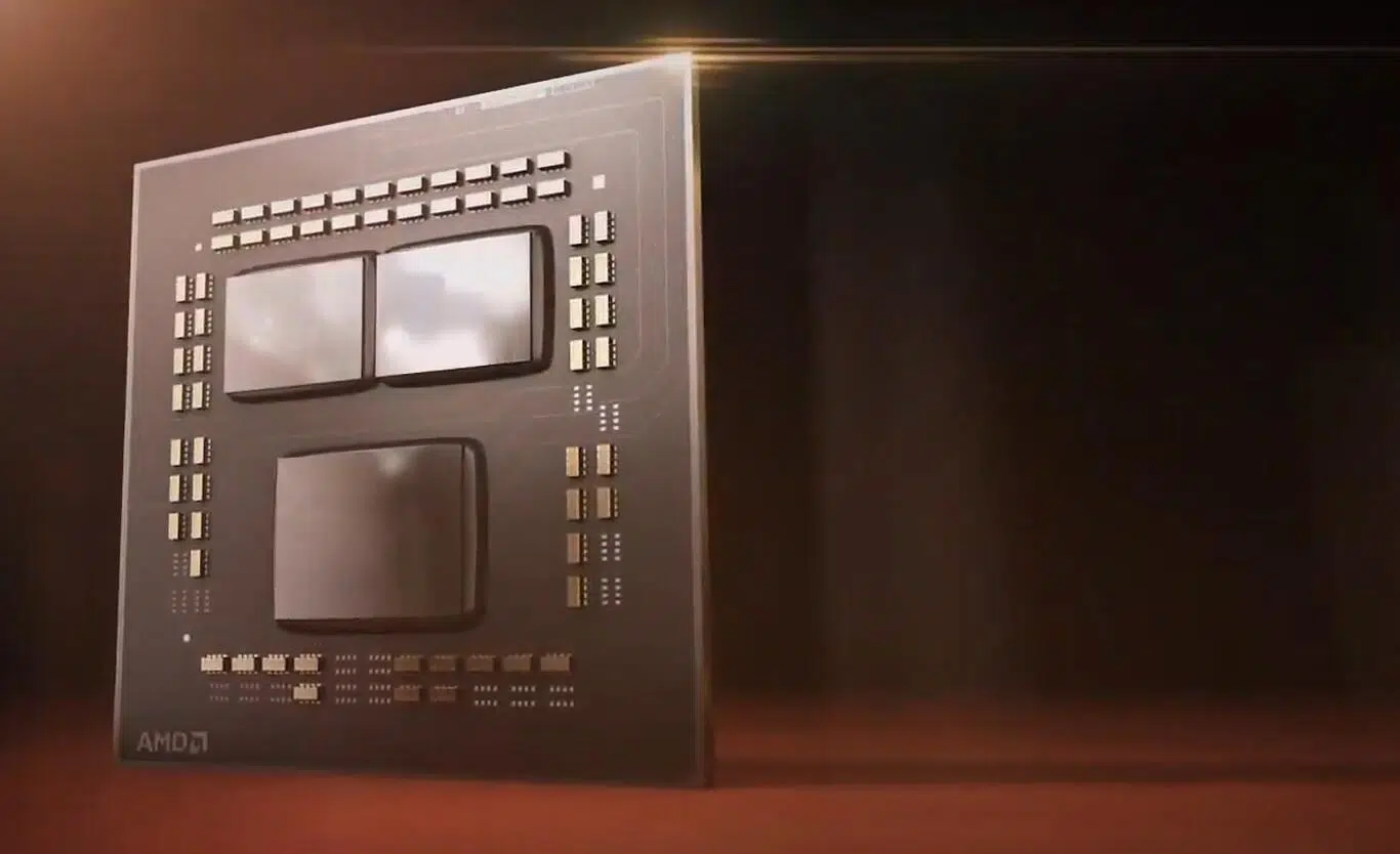
The microarchitecture of a CPU often takes a back seat to more eye-catching figures like GHz or MB of cache, but it is precisely there, in the internal design of the processor, where most of its real performance, its efficiency, and even what type of software can best take advantage of it are decided.
When you read technical specifications that mention cores, threads, L3 cache, or AVX2 , you're actually seeing the concrete consequences of a particular microarchitecture. Understanding how these components are organized internally, what makes a Zen 3 different from a Zen 2, or a hybrid Intel different from a classic Ryzen, is key to choosing your next CPU wisely and knowing why some excel in gaming, others in rendering, and still others in server tasks.
ISA, macroarchitecture and microarchitecture: bringing order to the concepts
Before delving into the complexities of pipelines and predictors, it's helpful to distinguish between three often-conflated levels: system macroarchitecture, ISA, and microarchitecture . Each describes a different layer of the computer.
On one hand, there's the macroarchitecture, or overall system design , which encompasses everything you see on the motherboard: CPU, memory controllers, buses, main memory, input/output chips, storage controllers, any external accelerators, and DMA logic. It's a high-level picture of how the large hardware components connect and how data flows between them.
Above that is the ISA (Instruction Set Architecture) , which is the instruction set that the processor understands: the types of data it handles, word size, number and type of registers, addressing modes, instruction formats, etc. When you program in assembly using mnemonics like ADD, SUB, MUL , or invoke extensions like SSE, AVX, or NEON, you are communicating directly with the ISA.
Finally, we have the microcode, or μISA , which defines the internal micro-operations that some complex architectures (like x86) use to implement their CISC instructions. This microcode can be updated via firmware to fix bugs or add support for new instructions.
What exactly is the microarchitecture of a CPU?
The CPU microarchitecture is essentially the internal blueprint that determines how ISA instructions are executed and how data moves within the chip. Two processors can share the same ISA (for example, AMD64 in Intel and AMD) and yet have radically different behavior and performance due to—or perhaps because of—their microarchitecture.
This design includes elements such as the type of control unit , whether programmable microcode or hardwired logic is used; the memory hierarchy; the depth of the pipeline; how many functional units work in parallel; and whether the processor is capable of executing instructions out of order and speculatively.
In addition, the designer must choose the pipeline depth : from simple CPUs without pipelining, where each instruction is processed from beginning to end before starting the next one, to modern designs with many stages (fetch, decode, rename, dispatch, execute, write-back, retire…) that allow dozens of instructions to be in flight at the same time.
Related to this is the number and type of execution units : ALUs for integers, multiplication units, dividers, FPUs for scalar and vector floating-point numbers, AGUs (Address Generation Units) for calculating memory addresses, jump units, etc. If there are several units of the same type, we speak of superscalar processors, capable of dispatching several instructions per cycle.
This is the basis for advanced techniques such as speculative execution , where the CPU anticipates the resolution of a branch and executes instructions from one of the branches in advance. If the prediction is correct, time is saved; if it fails, the work done is discarded and the pipeline is emptied, with the corresponding penalty.
Most modern high-performance CPUs also use out-of-order (OoO) execution . Instead of strictly adhering to the program order, the processor internally reorders instructions and executes first those whose data is ready, avoiding idle cycles while others wait for memory or the result of previous operations.
To make all this work without violating the program's semantics, register renaming is used . The compiler sees a limited set of logical registers, but the microarchitecture translates them into a larger bank of physical registers, dynamically assigning new destinations to break false dependencies and allow for greater parallelism.
Finally, the design can focus on adding parallelism at the core and thread level . This includes everything from single-core CPUs to chips with dozens or hundreds of cores (manycore), multiprocessor systems with multiple sockets interconnected by high-speed mesh networks (Infinity Fabric, Intel Mesh, NVLink, etc.), and simultaneous multithreading (SMT) support so that each physical core can handle two or more logical threads.
Compatibility, ISA and microarchitecture families
Since a microarchitecture is just one specific implementation of an ISA , a single ISA can have dozens of different microarchitectures over the years and across different manufacturers. This is precisely what happens with x86-64/AMD64 or ARM.
Looking solely at AMD within the AMD64 ISA, we find families as diverse as K8/Hammer, K10, Bulldozer, and the entire Zen series (Zen, Zen+, Zen 2, Zen 3, Zen 4...). They all execute the same basic instruction set, but their internal organization, caches, pipelines, and parallel execution approaches are completely different.
When we switch ISAs, the leap in compatibility is absolute. An ARM A64 -based processor (like Apple Silicon) cannot run binaries compiled for x86-64, and vice versa, unless a translation or emulation layer like Rosetta 2, QEMU, or similar is used, with the corresponding performance cost.
Even among processors that share an ISA, there's no guarantee they all support the same instruction set or extensions. An older chip might lack AVX2 or AVX-512, or an ARM SoC might implement only a subset of optional extensions. Therefore, a binary that heavily utilizes AVX-512 might fail to boot on a CPU that only offers SSE4.
When compiling software, it's common practice to generate generic binaries for a specific ISA (for example, x86-64 with at least SSE2) without fully utilizing any particular microarchitecture, so that the executable runs on as many CPUs as possible. However, if you compile with tuning flags for a specific microarchitecture (-march=znver3, -mtune=skylake, etc.), you can significantly improve performance on that particular family, at the cost of losing compatibility with others.
ISA licenses and intellectual property of the design
Not only is program code protected by licenses: ISAs and microarchitectures are also intellectual property. No one can legally clone an x86 or AMD64 ISA without a license, just as a proprietary CPU design cannot be copied without permission.
In the realm of ISAs, there are three main approaches. On one hand, there are closed ISAs , where the owner tightly controls who can implement compatible cores. The classic example is IA-32 (x86-32), historically owned by Intel, which granted licenses to AMD, VIA, and others, not without legal battles.
A similar situation exists with AMD64/x86-64 , initially designed by AMD and later licensed to Intel (which called it EM64T) through cross-licensing agreements. Other players, such as Hygon in China, have also obtained licenses for specific versions (for example, Zen 1 for the Chinese market).
Then we have ISAs with flexible licensing , where the owner offers both ISA licenses and ready-to-integrate IP cores. ARM, SPARC, or OpenPOWER fit here: you can pay to use Cortex A/M/R or Neoverse as is, or for a license that allows you to design your own microarchitectures on top of the ISA, as Apple does with its M1/M2/M3 or Qualcomm with its Kryo.
Finally, there are open-source ISAs , where anyone can create compatible microarchitectures without paying royalties for the ISA (although they can patent or close their own implementation). RISC-V is the best example: the ISA is under a permissive BSD license, and there are options ranging from completely open kernels in Verilog or Chisel to closed commercial designs.
In addition to the ISA, each specific microarchitecture (a Zen 4 core, a Cortex X4, a GPU design, etc.) is a block of patented or registered intellectual property. There are also open designs here, published as soft cores on HDL for synthesis in FPGAs or integration into custom SoCs.
Delving deeper into modern microarchitectures: the AMD Zen case
To see how all this translates into real-world performance, there's nothing like dissecting a specific product family. AMD has dramatically transformed its business thanks to Zen and its successive iterations , moving from the difficult Bulldozer era and the old FX processors to competing head-to-head (and sometimes even surpassing) Intel in desktop, server, and laptop markets.
After the failure of the AMD Fusion strategy , the company restructured and opted for a high-performance design led by, among others, Jim Keller. The Zen plan aimed to aggressively increase IPC (instructions per cycle) compared to Bulldozer, improve performance per watt, and regain ground in single-core performance, where Intel had held a lead for years.
One of the key changes was strengthening the front-end , the part responsible for fetching and preparing instructions. Zen introduced a micro-operation cache that stores already decoded micro-ops, similar to what some Intel microarchitectures like Conroe did. Bulldozer lacked this and relied more on the classic instruction cache hierarchy, which negatively impacted its throughput.
Zen's decoder can translate up to four CISC x86-64 instructions per cycle into RISC-like micro-ops. These micro-ops are then placed in a queue fed by the micro-op buffer, which in turn can dispatch up to six micro-ops per cycle to the back-end schedulers. This is where the out-of-order execution begins.
AMD clearly separated the integer and floating-point paths . On the integer side, ALUs, AGUs, and load/store logic are fed from the micro-ops queue. This logic is capable of performing two 16-byte loads and one 16-byte store per cycle from a 32 KB, 8-way L1D, with a write-back policy.
The floating-point and vector side feeds FMAC and AVX units. With two multiplication ports and two addition ports, Zen can simultaneously execute two 128-bit FMA operations or one 256-bit AVX operation per clock cycle. This instruction-level parallelism is one of the keys to its strong performance under computationally intensive workloads.
Cache hierarchy, TLB, and memory organization in Zen
The memory hierarchy in Zen is organized into three cache levels: separate L1 for instructions and data, private L2 per core, and shared L3 . Although it inherits the basic structure of previous microarchitectures, sizes, associativity, and policies have been refined.
The L1I (instruction cache) offers 64 KB per core, with 4 associative paths, doubling the number of paths per module compared to Bulldozer and reducing conflicts. The L1D (data cache) is increased to 32 KB, 8 paths, and a write-back policy, compared to Bulldozer's 16 KB, 4 paths, and write-through, significantly improving both hit rate and write efficiency.
The L2 cache is implemented as 512 KB per core and 8-way, instead of the 2 MB 16-way shared per module of the previous generation. The L3 cache, meanwhile, offers several MB per core set with 16-way associativity, acting as the last shared level before going to DRAM.
In parallel, Zen separates the TLBs into ITLBs (for instructions) and DTLBs (for data) , each with several levels and hundreds of entries, all with parity protection. This significantly reduces virtual-to-physical address translation latency, which becomes increasingly critical as memory sizes grow.
When we talk about a cache being 2-way, 4-way, or 8-way , we're describing its associativity, which is closely related to the idea of interleaving in memory. More associativity means more different ways to store a block of memory in that cache, reducing conflicts, but at the cost of slightly more complex logic and a slight increase in latency.
It's also important to understand the difference between write-through and write-back . In write-through, each write updates both the cache and main memory simultaneously, simplifying consistency but increasing traffic. In write-back, only the cache is written, and the line is marked with a dirty bit; the DRAM is only updated when that line is evicted, saving bandwidth and improving performance at the cost of slightly more complex logic.
Zen and Zen+: a leap in CPI and efficiency
Zen represented a very significant IPC leap for AMD compared to Bulldozer , thanks to the combination of a better front-end, a better branch predictor, more execution units, SMT instead of CMT (each full core handles two threads, instead of sharing part of the FPU between two logical cores) and a much more sensible cache hierarchy.
In addition to the design, AMD benefited from more advanced manufacturing processes with FinFET and smaller nodes , which allow for increased transistor density, reduced power consumption at the same performance, and higher frequencies while maintaining reasonable TDPs ( voltage-frequency curve ). This balance of performance per watt was crucial for regaining competitiveness in laptops and servers.
The transition from Bulldozer to Zen also brought longer retire queues, larger instruction schedulers, greater internal bandwidth, branch prediction with techniques based even on simple neural networks, and an SMT capable of better squeezing the available execution units.
In this context, Zen+ emerges , which we could see as the equivalent of a "tick" in Intel's old Tick-Tock strategy: the same basic design as Zen, but manufactured on a more refined node, with frequency improvements, slight latency reductions, and internal timing adjustments. It's not an architectural revolution, but rather a refinement that translates into a few extra performance points.
Zen 2: chiplets, full AVX2 and deep refinement
With Zen 2 , AMD is no longer just polishing the process: it's introducing substantial microarchitecture changes and massively launching its chiplet strategy . Instead of a single large monolithic die, it's dividing the design into several smaller 7nm compute dies (CCDs) and a separate 12nm I/O die handling memory, PCIe, and interconnects.
This chiplet approach improves yield per wafer (it's easier to manufacture small, defect-free dies), reduces costs, and makes it easier to scale the number of cores: simply add more CCDs to reach 16, 32, or more cores in EPYC and Threadripper. The trade-off is slightly more complex internal communication, dependent on the Infinity Fabric interconnect, which AMD has been refining generation after generation.
In terms of raw performance, AMD speaks of around +15% IPC for Zen 2 compared to Zen+ at the same frequency and an overall performance improvement per watt that can be around +75% compared to the first Zen when design and process improvements are combined.
In the vector back-end, Zen 2 takes the missing piece: it offers full 256-bit AVX2 support in a single micro-op , without splitting instructions into two 128-bit operations as was the case in Zen/Zen+. This means that the vector execution units are now truly 256-bit and can process AVX2 workloads at full speed with a much smaller frequency penalty than in other designs.
The micro-ops cache is also being reinforced, increasing to 4K entries (double its size), taking advantage of some of the area freed up by halving the L1I cache but doubling its associativity from 4 to 8 ways. Internal simulations led AMD to conclude that, for most real-world workloads, a larger uop cache is more advantageous than a larger L1I cache.
The L3 cache per core block is doubled in capacity , which helps reduce last-level failures, although access latency increases from approximately 35 to 40 cycles. To mitigate this effect, Zen 2 improves load and store bandwidths and refines the prefetch policy.
Another important aspect is the branch predictor. Zen 2 uses a TAGE (TAgged GEometric) predictor with over 7 entries, capable of leveraging variable-length histories and tagged entries. This reduces aliasing between different branches and, according to AMD, cuts the number of incorrect predictions by around 30% compared to the previous scheme, which directly translates to fewer pipeline flushes and higher IPC.
Zen 2 Back-end: AGUs, buffers, and adjusted latencies
In the entire back-end, Zen 2 continues to dispatch up to six micro-ops per cycle from the reorder buffer, which is expanded to approximately 224 entries (compared to Zen's 192). The scheduling units are divided into four queues for ALUs of 16 entries each and one queue for AGUs of 28 entries.
The number of Address Generation Units (AGUs) increases from two to three, although they are not all identical: two of them can handle both loads and writes, while the third specializes in storage operations. This distribution is designed for typical software profiles, where loads are usually more frequent and critical than store operations.
In the floating-point plane, the back-end can accept four micro-ops per cycle to its 256-bit FMA vector units, supported by a 160-entry physical register file. The 256-bit load/store paths have been improved to feed these units at a sustained rate under heavy vector workloads.
Zen 2 also adjusts the latencies of certain operations : for example, floating-point multiplication reduces its latency from 4 to 3 cycles, which helps with very tight numerical calculation loops. And, in general, there are a set of small optimizations spread throughout the pipeline that add up to that extra IPC seen in synthetic benchmarks and real-world applications.
Regarding the internal hierarchy by core groups, AMD uses the CCX (Core Complex) concept : a block of 4 cores that share the same L3 cache (16 MB in Zen 2). This extra size implies slightly higher latency, but in return reduces the failure rate, especially in applications with large working sets.
For reference, we can recall approximate internal latency figures: around 4 cycles for L1 , about 12 for L2, and around 40 cycles for L3. The key is to keep as much data as possible in L1/L2 and reduce traffic to L3 and DRAM , something that the microarchitecture and compilers work together to achieve.
Infinity Fabric: the glue used in chiplets and its impact on performance
One component not always associated with microarchitecture, but vital in Zen 2 and later, is Infinity Fabric . This proprietary bus acts as a communication "highway" between CCXs, CCDs, the I/O die, memory, and, in general, between all the blocks of the SoC.
Infinity Fabric is an evolution of HyperTransport , the high-speed bus that AMD pioneered years ago and which was also used by third parties such as NVIDIA, Cisco, Sun, and other members of the consortium. IF inherits the philosophy of scalable point-to-point links, but adapted to the needs of modern SoCs and CPU-GPU interconnection.
In Zen 2, AMD introduces IF2 , with support for PCIe 4.0 and a 512-bit internal bus between CCXs, double that of the first version. This translates into more effective bandwidth and an efficiency improvement that AMD estimates at around 27% compared to IF1, helping to mitigate the performance penalty of switching between chiplets.
Furthermore, the Infinity Fabric clock is partially decoupled from the DRAM clock , allowing the main memory to scale to higher frequencies in certain scenarios without necessarily forcing IF to keep pace, which offers more fine-tuning room for enthusiasts and system designers.
In server processors like EPYC , with four or more compute chiplets, Infinity Fabric is what makes it possible to connect all the dice together with almost complete topologies (180º rotations, direct links, etc.), achieving die-to-die bandwidths that can easily exceed 150 GB/s bidirectional depending on the speed of the DDR used.
The combination of a robust microarchitecture in each core , a scalable design using chiplets, and sufficiently fast interconnects allows AMD to assemble CPUs with 32, 64, or more cores with outstanding performance in highly parallel workloads, while maintaining competitive IPC per thread.
Ultimately, when you compare processors in gaming benchmarks, 3D rendering, massive compilation, or scientific simulation, GHz and core count figures only tell part of the story. What truly makes the difference is how the microarchitecture orchestrates internal execution , how it utilizes or wastes each clock cycle, and what trade-offs the manufacturer has made between latency, bandwidth, power consumption, and complexity.

Table of Contents
- 1 ISA, macroarchitecture and microarchitecture: bringing order to the concepts
- 2 What exactly is the microarchitecture of a CPU?
- 3 Compatibility, ISA and microarchitecture families
- 4 ISA licenses and intellectual property of the design
- 5 Delving deeper into modern microarchitectures: the AMD Zen case
- 6 Cache hierarchy, TLB, and memory organization in Zen
- 7 Zen and Zen+: a leap in CPI and efficiency
- 8 Zen 2: chiplets, full AVX2 and deep refinement
- 9 Zen 2 Back-end: AGUs, buffers, and adjusted latencies
- 10 Infinity Fabric: the glue used in chiplets and its impact on performance